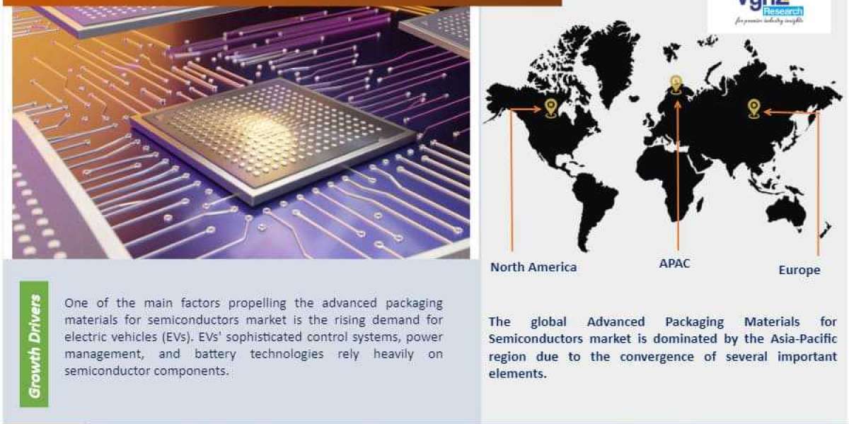
The world of semiconductors is ever-evolving, and at the heart of this evolution lies the global Advanced Packaging Materials for Semiconductors Market. According to VynZ Research, the market is poised to hit USD 59.00 billion by 2030, showcasing a robust Compound Annual Growth Rate (CAGR) of 7.02% during the forecast period from 2023 to 2030. This growth surge is fueled by the escalating demand for semiconductors across diverse industries like consumer electronics, automotive, and healthcare.
Get Sample Report for Free:
Key Market Trends
Rising Demand for Advanced Packaging Materials
The relentless pursuit of smaller, more powerful electronic devices has become a hallmark of the tech industry. To meet this demand, the market is witnessing a surge in the need for advanced packaging materials. These materials play a pivotal role in facilitating the miniaturization and integration of semiconductor components, ensuring that our devices become not only more compact but also more potent.
Shift to 3D Packaging
A notable trend in the semiconductor landscape is the significant shift towards 3D packaging. This approach involves stacking semiconductor dies on top of each other, a strategy that enhances performance while simultaneously reducing power consumption. The move to 3D packaging reflects the industry's commitment to pushing the boundaries of innovation and efficiency.
Growing Demand for Fan-Out Wafer-Level Packaging (FOWLP)
In the realm of advanced packaging, Fan-Out Wafer-Level Packaging (FOWLP) is emerging as a star player. This packaging type offers advantages in terms of cost, size, and performance. With these benefits, FOWLP is positioned to be the fastest-growing packaging platform in the years to come. Its flexibility and efficiency make it a go-to choice for semiconductor packaging.
Key Market Segments
By Material Type
The foundation of Advanced Packaging Materials for Semiconductors Market each with its unique properties. Silicones, copper, low-k dielectric, mold compounds, BT Resin (Bismaleimide Triazine), glass interposers, and solder materials constitute the key material types. Understanding the role and characteristics of each material is crucial for stakeholders navigating the advanced packaging landscape.
By Packaging Platform
Diving deeper into the market, the packaging platform becomes a focal point. Flip Chip, Embedded Die, Fan-in Wafer Level Packaging, and Fan-out Wafer Level Packaging (FOWLP) are the prominent packaging platforms. Each platform caters to specific needs, and grasping their applications is vital for making informed decisions in the semiconductor ecosystem.
By End-User
The end-user industries further define the landscape of advanced packaging materials. Consumer electronics, automotive, healthcare, and telecommunications stand out as key players. The unique requirements of each industry influence the choice of packaging materials, shaping the trajectory of the semiconductor market.
Key Market Players
In this dynamic market, several key players are steering the course of innovation and development. Companies such as Dow, DuPont, Henkel, Huntsman, Infineon Technologies, Intel, Merck, Shin-Etsu Chemical, Sumitomo Chemical, Teijin, and TSMC play pivotal roles. Their contributions, innovations, and market significance collectively shape the evolving narrative of advanced packaging materials for semiconductors.
Conclusion
The global advanced packaging materials for semiconductors market is on a trajectory of sustained growth, driven by technological demands and industry trends. The convergence of advanced packaging materials, 3D packaging, and the rise of FOWLP underscores the dynamic nature of the semiconductor landscape. As end-user industries evolve, so too will the requirements for innovative packaging solutions.
About Us
Global market research company, VynZ Research provides research, analytics, and consulting services for business plans. We provide specialized market research reports based on information that was predicted and estimated by industry professionals and experts. In addition to industry experts, the top-down and bottom-up approaches, data triangulation, and other techniques enable the market research leader to validate the data and deliver a major market study.
Contact Us:
Address: H.O - 9591 Fontainebleau Blvd. 617 Miami Florida 33172 U.S.A
Phone: +91 9960 288 381
Toll Free:1 888 253 3960
Email: marketing@vynzresearch.com
Website: www.vynzresearch.com