In the realm of high technology, where innovation and advancement reign supreme, silicon wafers play a pivotal role. These thin slices of silicon serve as the foundation for the production of integrated circuits, microchips, and various electronic components. At the heart of this intricate process are the diligent and specialized Silicon Wafer Manufacturers. We will delve into the fascinating world of silicon wafer manufacturing, exploring its significance, the manufacturing process, and the future of this vital industry.
The Significance of Silicon Wafers:
Silicon wafers are the building blocks of modern electronics. These wafers, typically made from highly purified polycrystalline or monocrystalline silicon, serve as the substrate upon which electronic components are built. Their unique electrical properties and reliability make them indispensable in the manufacturing of semiconductors.
- Enabling High-Performance Devices
Silicon wafers provide the necessary platform for the creation of high-performance devices. Their exceptional conductivity and ability to sustain high temperatures make them ideal for the demanding requirements of modern electronics. By facilitating the integration of complex circuits on a microscopic scale, silicon wafers enable the development of faster, smaller, and more efficient devices.
- Essential Component of Integrated Circuits
Integrated circuits (ICs) are the backbone of numerous electronic devices, from smartphones and computers to automobiles and medical equipment. Silicon wafers serve as the substrate for the fabrication of these ICs, allowing for the integration of transistors, resistors, capacitors, and other essential components. Without the precision and quality provided by silicon wafer manufacturers, the production of integrated circuits would be severely hindered.
- Fueling Technological Advancements
The relentless pursuit of technological advancements is fueled by silicon wafer manufacturers. As the demand for faster processors, higher storage capacities, and more sophisticated sensors continues to grow, silicon wafers become even more critical. Manufacturers constantly push the boundaries of wafer fabrication, striving to enhance performance, increase yield, and reduce costs. These ongoing efforts drive innovation across industries, revolutionizing sectors such as telecommunications, healthcare, automotive, and artificial intelligence.
The Silicon Wafer Manufacturing Process:
Silicon wafer manufacturing is a complex and highly precise process that involves several intricate steps. Each stage requires meticulous attention to detail and adherence to strict quality standards. Let us explore the key phases of this process:
- Silicon Ingot Growth
The manufacturing process begins with the growth of a silicon ingot. This step involves melting high-purity silicon in a quartz crucible at extremely high temperatures, typically in a vacuum or inert gas environment. Through controlled cooling, a solid cylindrical ingot is formed, which serves as the primary material for subsequent wafer production.
- Ingot Slicing
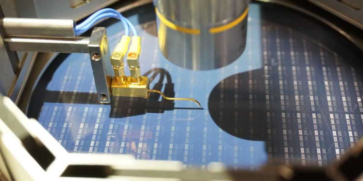
Once the silicon ingot has been grown, it undergoes slicing to create thin wafers. This step is carried out using advanced cutting techniques, such as wire sawing or diamond sawing. The ingot is carefully sectioned into thin slices, with the thickness depending on the desired application. These slices referred to as wafers, are then polished to achieve a smooth, mirror-like surface.
- Wafer Cleaning
To ensure the purity and quality of the wafers, thorough cleaning is essential. The wafers undergo a rigorous cleaning process, involving both chemical and mechanical techniques. Chemical cleaning removes any impurities or contaminants from the surface, while mechanical cleaning further enhances the cleanliness and smoothness of the wafers.
- Dopant Introduction
In order to impart specific electrical properties to the wafers, dopants are introduced. Dopants are impurity atoms that are strategically added to the silicon lattice. This process, known as doping, alters the electrical conductivity of the silicon, allowing for the creation of p-type and n-type regions. Doping is crucial for the formation of transistors and other semiconductor devices.
- Photolithography and Etching
Photolithography and etching are integral steps in the production of intricate circuit patterns on the wafer surface. A photosensitive material, called a photoresist, is applied to the wafer. A mask containing the desired circuit pattern is then aligned and exposed to ultraviolet light, transferring the pattern onto the wafer surface. The exposed areas are subsequently etched away, leaving behind the desired circuit structures.
- Thin Film Deposition
To create thin layers of various materials, thin film deposition techniques are employed. This process involves the controlled deposition of materials, such as silicon dioxide, silicon nitride, or metals, onto the wafer surface. Techniques like chemical vapor deposition (CVD) and physical vapor deposition (PVD) are used to achieve precise layer thickness and uniformity, enabling the creation of transistors, interconnects, and other components.
- Packaging and Testing
Once the desired circuitry has been fabricated on the wafer, the individual chips are separated through a process called dicing. These chips are then packaged, connecting them to external leads or pins. The packaged chips undergo rigorous testing to ensure their functionality and performance. This final stage ensures that only high-quality, reliable devices reach the market.
The Future of Silicon Wafer Manufacturing:
As technology continues to advance at an exponential rate, the future of silicon wafer manufacturing holds exciting possibilities. Here are a few areas that are likely to shape the future of this vital industry:
- Wafer Size Advancements
One key trend in silicon wafer manufacturing is the ongoing increase in wafer size. Over the years, the industry has witnessed a transition from smaller wafer diameters, such as 100 mm and 150 mm, to larger ones like 200 mm and 300 mm. The larger wafer size allows for more chips to be fabricated simultaneously, improving production efficiency and reducing costs. Further advancements, such as the development of 450 mm wafers, are being explored to accommodate the demands of future technologies.
- New Materials and Processes
To meet the evolving needs of the high-tech world, Silicon Wafer manufacturers are exploring alternative materials and processes. For instance, the introduction of compound semiconductors, such as gallium nitride (GaN) and silicon carbide (SiC), presents opportunities for higher power devices and better energy efficiency. Additionally, advanced manufacturing techniques like extreme ultraviolet lithography (EUV) are being researched to enable even finer circuit patterns and higher device densities.
- Semiconductor Packaging Innovations
The packaging of semiconductor devices is an area of continuous innovation. As devices become smaller and more complex, new packaging technologies are being developed to address the challenges of thermal management, power delivery, and interconnectivity. Advanced packaging techniques, such as 3D stacking, chiplets, and system-in-package (SiP), are expected to play a significant role in the future of silicon wafer manufacturing, enabling more compact and integrated electronic systems.
- Sustainability and Environmental Impact
With growing concerns about environmental sustainability, the silicon wafer manufacturing industry is actively working towards reducing its environmental footprint. Efforts are being made to minimize water and energy consumption, optimize material usage, and implement efficient waste management practices. Furthermore, research into greener alternatives for chemicals and processes is underway to mitigate the environmental impact of silicon wafer manufacturing.
Conclusion:
Silicon wafer manufacturers hold a crucial position in the high-tech world, enabling the production of advanced electronic devices that shape our lives. Their meticulous fabrication process, from ingot growth to final packaging, ensures the quality, reliability, and performance of integrated circuits and microchips. As technology continues to advance, silicon wafer manufacturing will evolve, embracing larger wafer sizes, new materials, innovative packaging techniques, and sustainable practices. The future of this industry holds immense potential, driving the next wave of technological breakthroughs and shaping the world of tomorrow.